| Sign In | Join Free | My wpc-board.com |
|
- Home
- Products
- About Us
- Quality Control
- Contact Us
- Get Quotations
| Sign In | Join Free | My wpc-board.com |
|
Brand Name : Hua Xuan Yang
Model Number : 5N60
Certification : RoHS、SGS
Place of Origin : ShenZhen China
MOQ : 1000-2000 PCS
Price : Negotiated
Payment Terms : L/C T/T Western Union
Supply Ability : 18,000,000PCS / Per Day
Delivery Time : 1 - 2 Weeks
Packaging Details : Boxed
Product name : Mosfet Power Transistor
APPLICATION : Power Management
FEATURE : Excellent RDS(on)
Power mosfet transistor : Enhancement Mode Power MOSFET
5N60 K-TCQ 5A 600V N-CHANNEL POWER MOSFET
The UTC 5N60K-TCQ is a high voltage power MOSFET and is designed to have better characteristics, such as fast switching time, low gate charge, low on-state resistance and have a high rugged avalanche characteristics. This power MOSFET is usually used at high speed switching applications in power supplies, PWM motor controls, high efficient DC to DC converters and bridge circuits.
FEATURES
RDS(ON) < 2.5Ω @ VGS =10V, ID = 2.5A
* Fast Switching Capability
* Avalanche Energy Specified
* Improved dv/dt Capability, High Ruggedness

Application
Load switching
Hard switched and high frequency circuits Uninterruptible power supply

| Ordering Number | Package | Pin Assignment | Packing | |||
| Lead Free | Halogen Free | 1 | 2 | 3 | ||
| 5N60KL-TA3-T | 5N60KG-TA3-T | TO-220 | G | D | S | Tube |
| 5N60KL-TF1-T | 5N60KG-TF1-T | TO-220F1 | G | D | S | Tube |
| 5N60KL-TN3-R | 5N60KG-TN3-R | TO-252 | G | D | S | Tape Reel |
Note: Pin Assignment: G: Gate D: Drain S: Source

ABSOLUTE MAXIMUM RATINGS (TC = 25°С, unless otherwise specified)
| PARAMETER | SYMBOL | RATINGS | UNIT | |
| Drain-Source Voltage | VDSS | 600 | V | |
| Gate-Source Voltage | VGSS | ±30 | V | |
| Drain Current | Continuous | ID | 5.0 | A |
| Pulsed (Note 2) | IDM | 20 | A | |
| Avalanche Current (Note 2) | IAR | 4.0 | A | |
| Avalanche Energy | Single Pulsed (Note 3) | EAS | 80 | mJ |
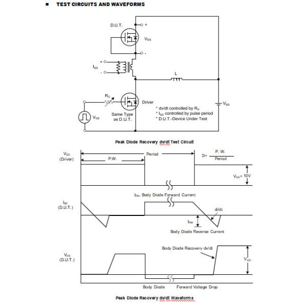
| Peak Diode Recovery dv/dt (Note 4) | dv/dt | 3.25 | V/ns | |
|
Power Dissipation | TO-220 |
PD | 106 | W |
| TO-220F1 | 36 | W | ||
| TO-252 | 50 | W | ||
| Junction Temperature | TJ | +150 | °C | |
| Storage Temperature | TSTG | -55 ~ +150 | °C | |
Notes: 1. Absolute maximum ratings are those values beyond which the device could be permanently damaged.
Absolute maximum ratings are stress ratings only and functional device operation is not implied.
4. Repetitive Rating: Pulse width limited by maximum junction temperature.
5. L = 84mH, IAS =1.4A, VDD = 50V, RG = 25 Ω Starting TJ = 25°C
6. ISD ≤ 2.0A, di/dt ≤200A/μs, VDD ≤BVDSS, Starting TJ = 25°C
| PARAMETER | SYMBOL | RATING | UNIT | |
| Junction to Ambient | TO-220F/TO-220F1 | θJA | 62.5 | °C/W |
| TO-252 | 110 | °C/W | ||
|
Junction to Case | TO-220 |
θJC | 1.18 | °C/W |
| TO-220F1 | 3.47 | °C/W | ||
| TO-252 | 2.5 | °C/W | ||
ELECTRICAL CHARACTERISTICS (TJ = 25°С, unless otherwise specified)
| PARAMETER | SYMBOL | TEST CONDITIONS | MIN | TYP | MAX | UNIT | |
| OFF CHARACTERISTICS | |||||||
| Drain-Source Breakdown Voltage | BVDSS | VGS=0V, ID=250μA | 600 | V | |||
| Drain-Source Leakage Current | IDSS | VDS=600V, VGS=0V | 1 | μA | |||
| Gate-Source Leakage Current | Forward | IGSS | VGS=30V, VDS=0V | 100 | nA | ||
| Reverse | VGS=-30V, VDS=0V | -100 | |||||
| ON CHARACTERISTICS | |||||||
| Gate Threshold Voltage | VGS(TH) | VDS=VGS, ID=250μA | 2.0 | 4.0 | V | ||
| Static Drain-Source On-State Resistance | RDS(ON) | VGS=10V, ID=2.5A | 2.5 | Ω | |||
| DYNAMIC CHARACTERISTICS | |||||||
| Input Capacitance | CISS |
VGS=0V, V DS=25V, f=1.0MHz | 480 | pF | |||
| Output Capacitance | COSS | 60 | pF | ||||
| Reverse Transfer Capacitance | CRSS | 6.5 | pF | ||||
| SWITCHING CHARACTERISTICS | |||||||
| Total Gate Charge (Note 1) | QG | VDS=50V, ID=1.3A, VGS=10V IG=100μA (Note 1, 2) | 46 | nC | |||
| Gate to Source Charge | QGS | 4.6 | nC | ||||
| Gate to Drain Charge | QGD | 6.0 | nC | ||||
| Turn-ON Delay Time (Note 1) | tD(ON) |
VDD=30V, VGS=10V, ID=0.5A, RG=25Ω (Note 1, 2) | 42 | ns | |||
| Rise Time | tR | 44 | ns | ||||
| Turn-OFF Delay Time | tD(OFF) | 120 | ns | ||||
| Fall-Time | tF | 38 | ns | ||||
| SOURCE- DRAIN DIODE RATINGS AND CHARACTERISTICS | |||||||
| Maximum Body-Diode Continuous Current | IS | 5 | A | ||||
| Maximum Body-Diode Pulsed Current | ISM | 20 | A | ||||
| Drain-Source Diode Forward Voltage (Note 1) | VSD | IS=5.0A, VGS=0V | 1.4 | V | |||
| Body Diode Reverse Recovery Time (Note 1) | trr | IS=5.0A, VGS=0V, dIF/dt=100A/μs | 390 | nS | |||
| Body Diode Reverse Recovery Charge | Qrr | 1.6 | μC | ||||
Notes: 1. Pulse Test : Pulse width ≤ 300µs, Duty cycle ≤ 2%.


|
|
5N60 K-TCQ 5A 600V N-CHANNEL POWER MOSFET Images |